本节包括SPI配置DAC芯片实例、异步并口通信等。
SPI配置时序
1.某DAC芯片的SPI配置时序
- 此时时序的关键是:时钟上升沿主机给从机发数据,时钟下降沿从机给主机发数据
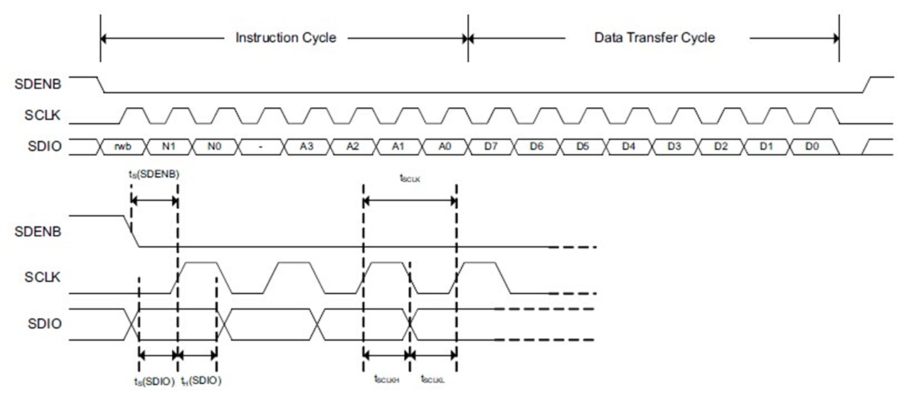
正因如此,利用FPGA的系统时钟产生SPI的分频时钟后,需要进行180°时钟反相,也就是用产生的分频时钟去控制SPI的配置时序,但最终输出的SPI实际时钟是分频时钟的180°反相,这样能使得SPI上要发送的数据正好处于SPI时钟的上升沿

并且,关于DAC的配置,总共需要发送32个16bit的数据才算完成,此处牵扯到串行处理,故用状态机控制
2.源代码
1 |
|
3.Testbench
1 |
|
结果如下:
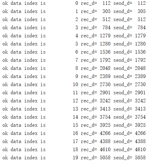
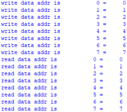
这里写测试代码的方式值得一学,不然还得人工判断传输的结果是否正确
1
2
3
4
5
6
7
8
9
10
11
12
13
14
15
task rec_spi();
integer i,j;
begin
for (i=0;i<32;i=i+1)begin
for(j=0;j<16;j=j+1)begin
@(posedge spi_clk);
shift_buf = {shift_buf[14:0],spi_sdi};
if(j==15 && shift_buf == send_mem[i])
$display("ok data index is %d rec_d=%d send_d=%d",i,shift_buf,send_mem[i]);
else if(j== 15)
$display("error");
end
end
end
endtask
4.Reference
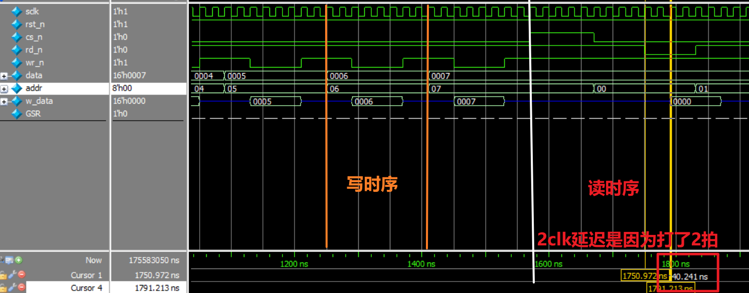
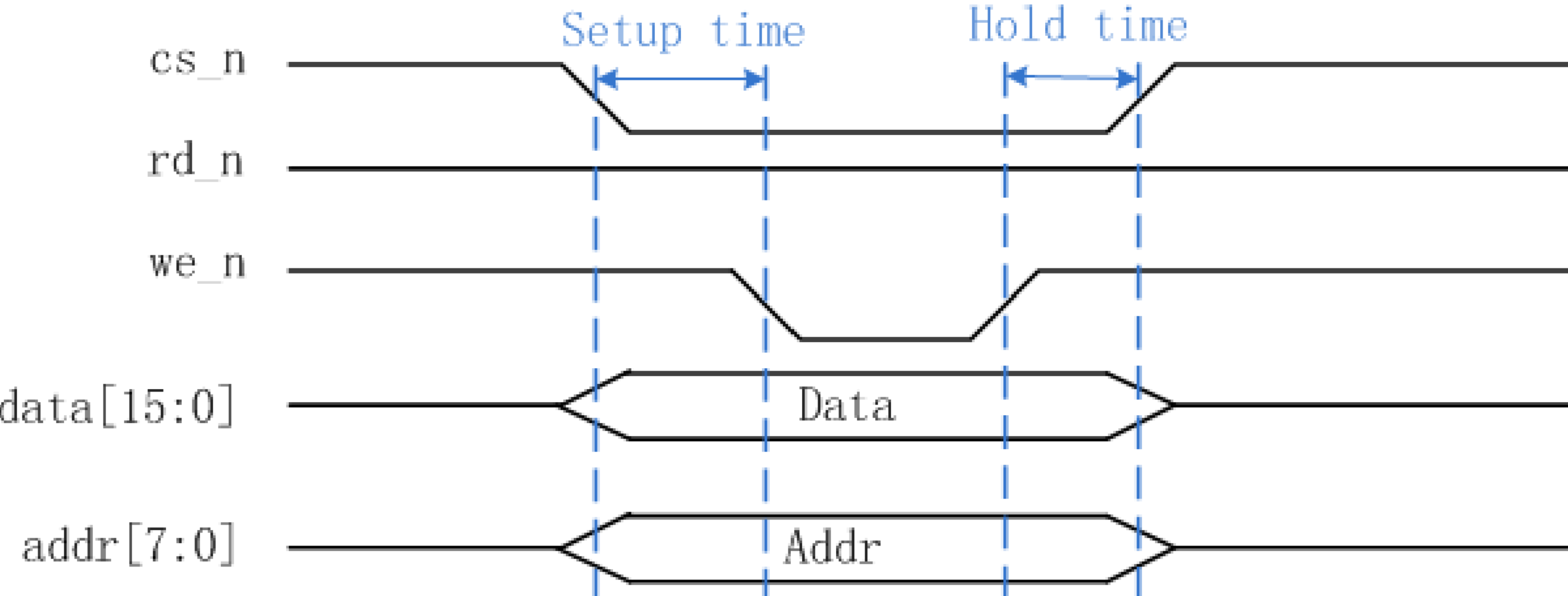
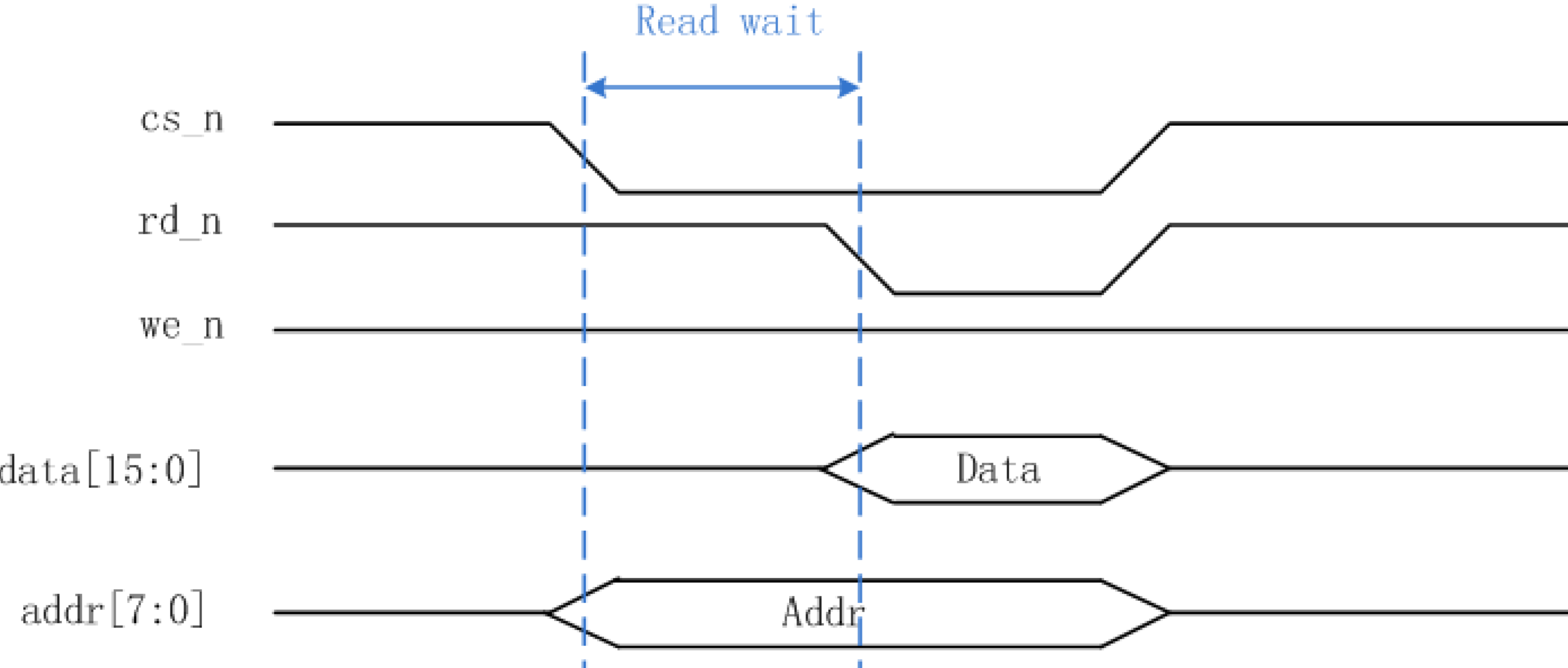
异步并口通信
异步并口应用:CPU类的芯片与FPGA的数据交互,数据速率一般在100Mbps以内,数据总线不大于16bit
写操作(外部芯片对FPGA写)的时序图:
读操作(外部芯片读FPGA内数据)时序图:
1.源代码
1 |
|
2.Testbench*
- testbench的测试方式值得学习,其实就根据时序图给出每个时序信号就可
1 |
|
仿真结果: